| Ultra Products 1024MB PC3200 XL Dual Channel DDR - Page 2 of 3 |
Test Setup:
The test machine used in this review consisted of the following components:
DFI nForce4 Ultra-D Motherboard
AMD A64 3000+ (939) Winchester Core Processor
Sapphire X850XT Video Card
Thermaltake PIPE101 cooler
Western Digital Raptor Hard Drive
Seagate 120 Gig SATA Drives in RAID 1
Windows XP Pro SP1, all current updates and drivers installed
All testing was done with the following settings:
DFI Bios 310
CPU multiplier @ 7
PCI/AGP bus locked at 66 Mhz
Average processor temperature is 35 to 38c
CPU Voltage 1.50v
Command Per Clock (CPC) at 2T (Disabled)
Ratio set at 1:1 CPU/ Memory Frequency
Testing:
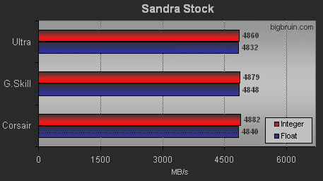
First off I wanted to find the ceiling to the Ultra Products XL DDR at the default SPD timings. Starting with the default SPD settings at 200 MHz and 2.6 volts, I ramped up the FSB and could only reach 206 MHz Memtest error free. The Corsair and G. Skill memory produced the same results. Keep in mind this is with no changes in the BIOS at all. The charts below shows the results from the Sisoft Sandra memory benchmark at SPD timings and 200 MHz.

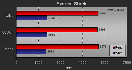
The charts below shows the Read/write bandwidth results from Everest at SPD timings and 200 MHz.

With that information, it was time to loosen the timings and see how high I could go. After a few hours of playing with all of the available memory timings of the DFI Ultra-D motherboard, I found a set of timings that seemed to work well. These timings are rather loose and with more time, I think they could be tightened up somewhat.
DRAM timings from Bios:
CPC - (Command Per Clock) - Disabled
Tcl - (CAS Latency Control) - 2.5
Trcd - (RAS to CAS Delay) - 4 clocks
Tras - (Min RAS Active Time) - 7 clocks
Trp - (Row Precharge Time) - 3 clocks
Trc - (Row cycle Time) - 7 clocks
Trfc - (Row Refresh Cyc Time) - 14 clocks
Trrd - (Row to Row Delay) - 2 clocks
Twr - (Write Recovery Time) - 3 clocks
Twtr - (Write to Read Delay) - 2 clocks
Trwt - (Read to Write Delay) - 4 clocks
Tref - (Refresh Period) - 3072 Cycles
Twcl - (Write CAS Latency) - 1 clock
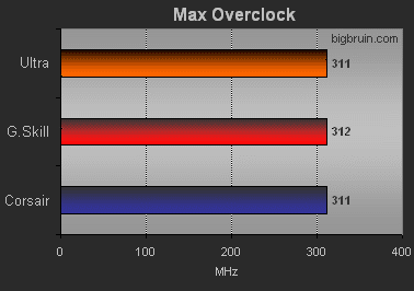
With the above timings I started raising the FSB while keeping the stock memory voltage of 2.6 Volts. Having already found the ceiling of my disappointing Winchester core CPU (~2200MHz) I also lowered the multiplier to 7 to keep the effects of the processor out of the loop. I started to receive MemTest errors right around 250Mhz (PC4000, 500MHz DDR). After raising the voltage up to 2.8 Volts I was able to get clear up to 311 MHz, get into Windows and only have minor MemTest errors. Strangely enough, raising the voltage to 3.0 Volts didnt help any. Going to 3.2 Volts worsened the situation considerably. The TCCD based Ultra doesnt seem to be as voltage hungry as some of the older chips were. The chart below shows how each pair of memory faired in the maximum overclocking test at 2.8V.

Please read on to the next page for more... Next
Page 1 | Page 2 | Page 3 | Home | Forum | Review Index
|
|
|
|